| |
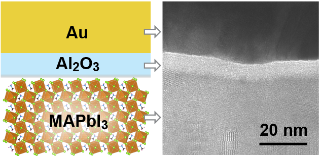
- J. Gong, et. al. “Nanoscale Encapsulation of Hybrid Perovskites Using Hybrid Atomic Layer Deposition”, J. Phys. Chem. Lett., 13, 4082 (2022). [link]
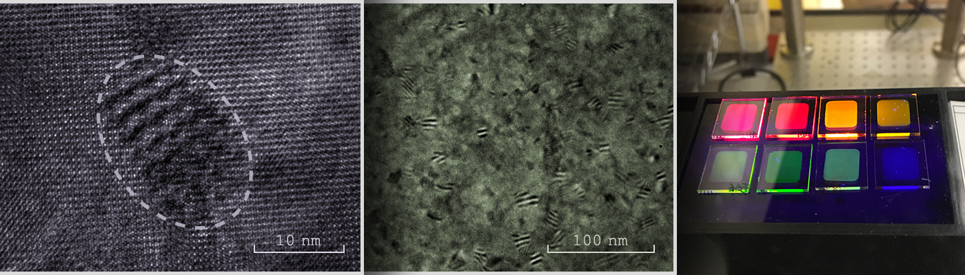
- Y. Wang, et. al. “Phase segregation in inorganic mixed-halide perovskites: from phenomena to mechanisms”, Photon. Res., 8, A56 (2020). [link]
- X. Wang, X. Lian, Z. Zhang, H. Gao, “Could Nanocomposites Continue the Success of Halide Perovskites?”, ACS Energy Lett., 4, 1446 (2019). [link]
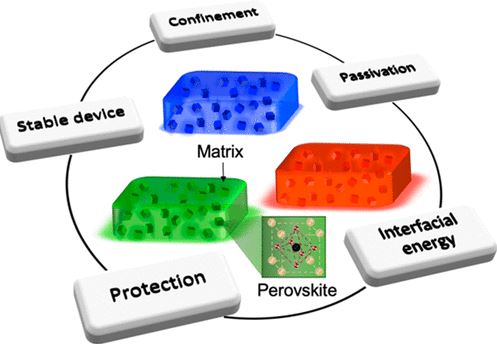
- X. Wang, et. al. “Suppressed Phase Separation of Mixed-Halide Perovskites Confined in Endotaxial Matrices”, Nat. Comm., 10, 695 (2019). [link]
- X. Lian, X. Wang, Y. Ling, E. Lochner, L. Tan, Y. Zhou, B. Ma, K. Hanson, H. Gao, “Light Emitting Diodes Based on Inorganic Composite Halide Perovskites”, Adv. Func. Mater., 29, 1807345 (2019). [link]
- Z. Chen, et. al. “Remote Phononic Effects in Epitaxial Ruddlesden–Popper Halide Perovskites”, J. Phy. Chem. Lett., 9, 6676 (2018). [link]
- Y. Tian, C. Zhou, M. Worku, X. Wang, Y. Ling, H. Gao, Y. Zhou, Y. Miao, J. Guan, B. Ma, “Highly Efficient Spectrally Stable Red Perovskite Light‐Emitting Diodes”, Adv. Mater., 30, 1707093 (2018). [link]
- Y. Ling, L. Tan, X. Wang, Y. Zhou, Y. Xin, B. Ma, K. Hanson, H. Gao, “Composite Perovskites of Cesium Lead Bromide for Optimized Photoluminescence”, J. Phy. Chem. Lett., 8, 3266 (2017). [link]
- X. Wang, et. al. “Dynamic Electronic Junctions in Organic-Inorganic Hybrid Perovskites”, Nano Lett., 17, 4831 (2017). [link]
- Z. Chen, Y. Wang, X. Sun, Y. Guo, Y. Hu, E. Wertz, X. Wang, H. Gao, T.-M. Lu, J. Shi, “Van Der Waals Hybrid Perovskite of High Optical Quality by Chemical Vapor Deposition”, Adv. Optical Mater., 1700373 (2017). [link]
- Y. Ling, et. al. “Enhanced Optical and Electrical Properties of Polymer-Assisted All-Inorganic Perovskites for Light-Emitting Diodes”, Adv. Mater., 28, 8983 (2016). [link]
- Y. Tian, Y. Ling, Y. Shu, C. Zhou, T. Besara, T. Siegrist, H. Gao, B. Ma, “A Solution-Processed Organometal Halide Perovskite Hole Transport Layer for Highly Efficient Organic Light-Emitting Diodes”, Adv. Electron. Mater., 2, 1600165 (2016). [link]
- S. R. Bade. et. al. “Fully Printed Halide Perovskite Light-Emitting Diodes with Silver Nanowire Electrodes”, ACS Nano, 10, 1795 (2016). [link]
- Y. Ling, Z. Yuan, Y. Tian, X. Wang, J. C. Wang, Y. Xin, K. Hanson, B. Ma, H. Gao, “Bright Light-Emitting Diodes Based on Organometal Halide Perovskite Nanoplatelets”, Adv. Mater., 28, 305 (2016). [link]
- X. Wang, H. Gao, “Distinguishing the Photothermal and Photoinjection Effects in Vanadium Dioxide Nanowires”, Nano Lett., 15, 7037 (2015). [link]
- B. Ashley, D. D. Lovingood, Y.-C. Chiu, H. Gao, J. Owensb, G. F. Strouse, “Specific effects in microwave chemistry explored through reactor vessel design, theory, and spectroscopy”, Phys. Chem. Chem. Phys., 17, 27317 (2015). [link]
- A. Fu, H. Gao, P. Petrov, and P. Yang, “Widely Tunable Distributed Bragg Reflectors Integrated into Nanowire Waveguides”, Nano Lett., 15, 6909 (2015). [link]
- Z. Chen, X. Lan, Y-C. Chiu, X. Lu, W. Ni, H. Gao, Q. Wang, “Strong Chiropitcal Activities in Gold Nanorod Dimers Assembled using DNA Origami Templates”, ACS Photonics, 2, 392 (2015). [link]
- N. P. Dasgupta, J. Sun, C. Liu, S. Brittman, S. C. Andrews, J. Lim, H. Gao, R. Yan, P. Yang, “Semiconductor Nanowires: Synthesis, Characterization, and Applications”, Adv. Mater., 26, 2137 (2014).
- H. Gao, A. Fu, S. Andrews, and P. Yang, “Cleaved-Coupled Nanowire Lasers”, Proc. Natl. Acad. Sci., 110, 865 (2013).
- J. Vura-Weis, C. Jiang, C. Liu, H. Gao, J. M. Lucas, F. M.F. de Groot, P. Yang, A. P. Alivisatos, S. R. Leone, “Femtosecond M2,3-edge spectroscopy of transition metal oxides: photoinduced oxidation state change in α-Fe2O3”, J. Phys. Chem. C Lett., 4, 3667 (2013).
- C. Hahn, A. A. Cordones, S. C. Andrews, H. Gao, A. Fu, S. R. Leone, and P. Yang, “Effect of Thermal Annealing in Ammonia on the Properties of InGaN Nanowires with Different Indium Concentrationss”, J. Phys. Chem. C, 117, 3627 (2013).
- H. Gao, C. Liu, H. E. Jeong, and P. Yang, “Plasmon Enhanced Water Splitting Efficiency of Iron Oxide on Au Nanopillars”, ACS Nano, 6, 234 (2012).
- G. Kichin, T. Weiss, H. Gao, J. Henzie, T.W. Odom, S.G. Tikhodeev, and H. Giessen, "Metal-dielectric Photonic Crystal Superlattice: 1D and 2D Models and Empty Lattice Approximation." Physica B: Condensed Matter 407, 4037 (2012).
- S. Brittman*, H. Gao*, E. C. Garnett, and P. Yang, “Absorption of Light in a Single-nanowire Silicon Solar Cell Decorated with an Octahedral Silver Nanocrystal”, Nano Letters, 11, 5189 (2011).
- D. Gargas*, H. Gao*, H. Wang, and P. Yang, “High Quantum Efficiency of Band-Edge Emission from ZnO Nanowires”, Nano Letters, 11, 3792 (2011).
- J. Tang, Z. Huo, S. Brittman, H. Gao, and P. Yang, “Solution processed core-shell nanowires for efficient photovoltaic cells”, Nature Nanotechnology, 6, 568 (2011).
- J. Y. Lin, J.-C. Yang, H. Gao, and T. W. Odom, “Surface Plasmon Biosensing with 3D Plasmonic Crystals”, Plasmonics and Plasmonic Metamaterials, G. Shvets, and I. Tsukerman, Eds (World Scientific Publishing Co. Inc.) ISBN 9789814355278 (2011).
- H. Gao, J. K. Hyun, M. H. Lee, J.-C. Yang, L. J. Lauhon, and T. W. Odom, “Broadband Plasmonic Microlenses Based on Patches of Nanoholes”, Nano Letters, 10, 4111 (2010).
- H. Gao, J.-C. Yang, J. Y. Lin, A. D. Stuparu, M. H. Lee, M. Mrksich, and T. W. Odom, “Using the Angle-Dependent Resonances of Molded Plasmonic Crystals To Improve the Sensitivities of Biosensors”, Nano Letters, 10, 2549 (2010).
- J.-C. Yang, H. Gao, J. Y. Suh, W. Zhou, M. H. Lee, and T. W. Odom, “Enhanced Optical Transmission Mediated by Localized Plasmons in Anisotropic, Three-Dimensional Nanohole Arrays”, Nano Letters, 10, 3173 (2010).
- H. Gao, W. Zhou, and T. W. Odom, “Plasmonic Crystals: A Platform to Catalog Resonances from Ultraviolet to Near-infrared Wavelengths in a Plasmonic Library”, Advanced Functional Materials, 20, 529 (2010) [Feature Article, Cover Story].
- W. Zhou, H. Gao, and T. W. Odom, “Toward Broadband Plasmonics: Tuning Dispersion in Rhombic Plasmonic Crystals”, ACS Nano, 4, 1241 (2010).
- T. W. Odom, H. Gao, J. McMahon, J. Henzie, and G. Schatz, “Plasmonic Superlattices: Hierarchical Subwavelength Hole Arrays”, Chemical Physics Letters 483, 187 (2009) [Frontiers Article, Cover Story]
- M. H. Lee, H. Gao, and T. W. Odom, “Refractive Index Sensing Using Quasi One-Dimensional Nanoslit Arrays”, Nano Letters 9, 2584 (2009).
- H. Gao, J. McMahon, M. H. Lee, J. Henzie, S. K. Gray, G. C. Schatz, and T. W. Odom, "Rayleigh Anomaly-Surface Plasmon Polariton Resonances in Palladium and Gold Subwavelength Hole Arrays”, Optics Express, 17, 2334 (2009).
- H. Gao, J. Henzie, M. H. Lee, and T. W. Odom, “Screening Plasmonic Metamaterials Using Pyramidal Gratings”, Proc. Natl. Acad. Sci., 105, 20146 (2008).
- H. Gao, and T. W. Odom, “Near-Field Optical Characterization of Plasmonic Materials”, Nano-Optics and Near-Field Optical Microscopy, A. Zayats, and D. Richards, Eds (Artech House, Inc., Norwood) ISBN 9781596932838 (2008).
- M. H. Lee, H. Gao, J. Henzie, and T. W. Odom, “Microscale Arrays of Nanoscale Holes”, Small 3, 2029 (2007).
- H. Gao, J. Henzie, and T. W. Odom, "Direct Evidence for Surface Plasmon-Mediated Enhanced Light Transmission through Metallic Nanohole Arrays", Nano Letters 6, 2104 (2006).
|
|
|